ED-7-1-INV
Design of on-chip lumped element bandpass filters for multichroic imaging in submillimeter astronomy
09:00-09:30 30/11/2023
*Shinsuke Uno1,2, Kah Wuy Chin1, Tai Oshima2,3, Satoshi Ono4, Takeshi Sakai4, Akira Endo5, Kenichi Karatsu5,6, Jochem J. A. Baselmans5,6, Tatsuya Takekoshi7, Kotaro Kohno1, Shuhei Inoue1,2, Toyo Naganuma2,4, Yuka Niwa8, Ryosuke Yamamura2,4, Kazuki Watanabe3
1. Institute of Astronomy, The University of Tokyo, 2-21-1 Osawa, Mitaka, Tokyo 181-0015, Japan
2. National Astronomical Observatory of Japan, 2-21-1 Osawa, Mitaka, Tokyo 181-8588, Japan
3. Department of Astronomical Science, The Graduate University for Advanced Studies (SOKENDAI), 2-21-1 Osawa, Mitaka, Tokyo 181-8588, Japan
4. Graduate School of Informatics and Engineering, The University of Electro-Communications, 1-5-1 Chofugaoka, Chofu, Tokyo 182-8585, Japan
5. Faculty of Electrical Engineering, Mathematics and Computer Science, Delft University of Technology, Mekelweg 1, 2628 CD Delft, The Netherlands
6. Netherlands Institute for Space Research (SRON), Niels Bohrweg 4, 2333 CA Leiden, The Netherlands
7. Kitami Institute of Technology, 165 Koen-cho, Kitami, Hokkaido 090-8507, Japan
8. Tokyo Institute of Technology, 2-12-1 Ookayama, Meguro-ku, Tokyo 152-8551, Japan
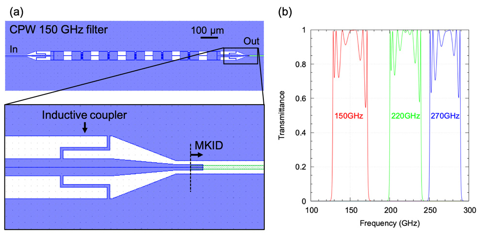
Band selection by on-chip filters coupled with superconducting photon detectors such as TES’s and MKIDs [1] is a key technology for multichroic imaging in millimeter/submillimeter astronomy. We report on the design of on-chip bandpass filters coupled to quarter-wave MKIDs for three frequency bands centered at 150, 220, and 270 GHz, each with a bandwidth of 40 GHz. We choose a lumped-element Chebyshev filter design to take advantage of its compactness and wide bandwidth [2,3]. Our design has inductive couplers or shunt inductance elements at the end of filters [Figure (a)], which allows efficient coupling to the absorbing part of a quarter-wave MKID resonator without any intermediate components. We find optimal designs using coplanar waveguide (CPW) and microstrip line structures based on the following method: First, we model each on-chip filter as an equivalent circuit of a Chebyshev bandpass filter, which consists of lumped inductors and capacitors, for a given set of center frequencies and bandwidths. Next we design planar inductors and capacitors with identical S-parameters as the lumped element inductors and capacitors in our equivalent model using planar electromagnetic simulations. Finally, we construct the entire filter by replacing lumped elements in the equivalent circuit with the corresponding planar structures. We use superconducting NbTiN films to construct the filters, which is modeled as a zero-thickness superconductor with a sheet inductance of 1 pH/sq and no resistance. Figure (b) shows the simulated spectral response of our optimal CPW filter designs, which covers the targeted bands. We will also present the results of electromagnetic simulations performed to evaluate the radiation loss as well as the S-parameters of our filter designs.
Figure (a): Design of the on-chip bandpass filter with CPW structures for 150 GHz.
Figure (b): Simulated transmissions of the CPW bandpass filters for three frequency bands.
[1] Mauskopf, P. D. (2018) PASP, 130, 082001
[2] Pozar, D. M. (2011) “Microwave Engineering,” John Wiley & Sons
[3] Suzuki, A. et al. (2012) J. Low Temp. Phys., 167, 852-858
This work was supported by JSPS KAKENHI Grant Number 22KJ0583.