ED-7-5
Superconducting Tunnel Junction X-ray Detectors on SiO2/SiN/SiO2 Membrane to reduce Substrate Noise
10:15-10:30 30/11/2023
*Tsuyoshi Noguchi1,2, Go Fujii2, Shigetomo Shiki2, Taiga Shibasaki1, and Tohru Taino1
1. Graduate School of Science and Engineering, Saitama University 255 Shimo Okubo, Sakura-ku, Saitama, 338-0815 Japan
2. Device Technology Research Institute, National Institute of Advanced Industrial Science and Technology Tsukuba No.2 Office 1-1-1 Umezono, Tsukuba-shi, Ibaraki, 305-8568 Japan
In recent years, renewable energy generation such as solar power and wind power, and electric vehicles have been attracting attention in order to reach a sustainable society. These products mainly use semiconductors based on silicon, but they are unable to satisfy desirable performance requirements in the future because of its material characteristics. Therefore, next-generation semiconductors such as SiC and GaN are attracting attention as alternative materials to Si. Material analysis using characteristic X-rays is an indispensable technology in the development of these next-generation semiconductors. Although X-ray spectra are generally measured by semiconductor detectors like silicon drift detectors (SDDs) in the analysis, it is difficult to clearly separate soft X-ray peaks generated from the next-generation semiconductors and dopants. On the other hand, superconducting tunnel junction (STJ) detectors have several times better the energy resolution than semiconductor detectors one. In fact, we have succeeded in XAFS analysis of N dopants (300 ppm) in n-SiC for the first time in the world [1].
Since the film thickness of STJs is usually very thin (several hundred nm), part of the high-energy X-rays penetrate the STJs and are absorbed in a Si substrate with a thickness of several hundred μm. The X-rays absorbed in the substrate generate many phonons, the phonons arriving at the STJ generate a charge signal of the STJ. This is the phonon noise at the STJ. The charge signal generated by the phonon noise is comparable to the signal charge generated by low-energy X-rays directly absorbed in the superconducting electrode. Therefore, the detection limit for dopant analysis in SiC and GaN is determined by this phonon noise.
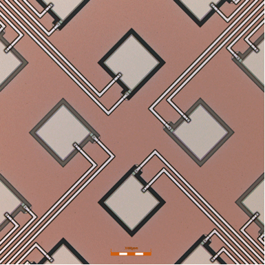
In order to reduce of the phonon noise, we fabricated Nb/Al STJs with 100 μm square on free-standing membrane without the Si substrate. The free-standing membrane consists of a three-layer structure of SiO2/SiN/SiO2. The phonon noise for Al-Kα was reduced to about 1/10 by using the structure. In addition, the energy resolution of the STJ is 9.7 eV, which is the best energy resolution among STJs operating at 0.3 K.
[1] S.Shiki, et al, J. Low Temp. Phys., vol 167, pp 748-753 , (2012).
A part of This work was supported by "Advanced Research Infrastructure for Materials and Nanotechnology in Japan (ARIM)" of the Ministry of Education, Culture, Sports, Science and Technology (MEXT). Proposal Number JPMXP1222AT5008.