WB-8-4
Induction of substrate-induced pinning centers in YBCO films with nanocomposite buffer layer
13:45-14:00 30/11/2023
*Shin Okumura, Tomoya Horide, Yutaka Yoshida
Nagoya University, Nagoya, Japan
Introduction
To increase critical current density(Jc) of YBa2Cu3O7-δ(YBCO) superconducting thin films, artificial pinning center(APC) such as BaMO3(BMO, M = Zr, Hf, Sn, etc.) are incorporated into YBCO films. BMO nanoparticles and nanorods are effective pinning centers, but the incorporation of second phase materials like BMO degrades the YBCO matrix. The difference of lattice parameter results in distortion at the interface between YBCO and BMO. In addition, the nanorod morphology is not stable, such as uneven distribution or deformation, in the case of large BMO content. The introduction of APCs without using second phase material should be discussed for further Jc improvement. Substrate-induced pinning centers in YBCO thin films has been reported [1,2]. The density of substrate-induced pinning is low in the previous reports, and higher density is needed to improve the Jc in high magnetic field. Therefore, we focus on the structure of buffer layer, which affects the initial stage of YBCO growth. Both SrTiO3(STO) and CeO2 are used as the buffer layer for YBCO growth, and it has been reported that nanoscale structure can be fabricated in the nanocomposite of STO and CeO2 [3]. Therefore, we investigated the pinning centers induced by the nanocomposite buffer layer of STO and CeO2 to introduce high density of substrate-induced pinning centers.
Experimental method
We prepared YBCO thin films on the STO and CeO2 nanocomposite buffer layer by using Pulsed Laser Deposition(PLD) method. MgO was used as the substrate. The volume percentage of STO:CeO2(STO:CeO2ratio) was changed to control the structure of buffer layer, and the X:100-X film denotes the YBCO film deposited on the buffer layer with the STO:CeO2 ratio of X:100-X. We used Dynamic Force Mode(DFM) of Atomic Force Microscope(AFM) to observe the surface roughness of the buffer layer. Energy dispersive X-ray spectroscopy(EDX) was used to evaluate the atomic fraction. Using X-Ray Diffraction(XRD), the phase formation and film orientation were evaluated. We also measured critical temperature(Tc) and Jc in the temperatures of 20 K~77 K and magnetic field of 0 T-9 T.
Experimental results and discussion
STO n00 and CeO2 n00 peaks in XRD 2θ-ω scan were observed in the YBCO/(STO, CeO2)/MgO thin films. The φ-scan shows that STO grows with the cube-on-cube orientation relationship. On the other hand, CeO2 has two types of orientation relationships of the cube-on-cube orientation and the 45-degree rotated orientation. The X-ray intensity ratio of the cube-on-cube orientation increases with an increase in the volume fraction of CeO2. This shows that the crystalline defects such as grain boundaries were successfully controlled by changing the STO:CeO2 ratio.
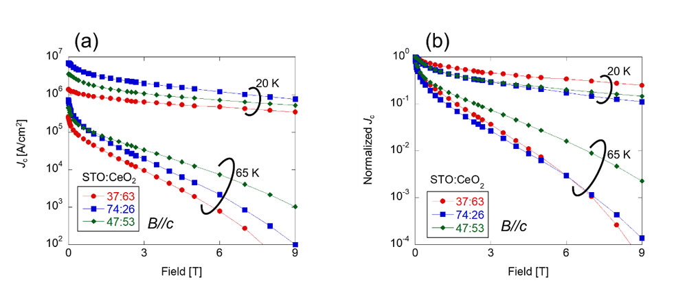
Fig.1(a) shows Jc-B characteristics at 65 K and 20 K in 0-9 T. Regardless of temperature, the 74:26 film has the highest Jc,self. However, Tc was 76.9 K for the 37:63 sample, 79.7 K for the 74:26 sample, and 81.3 K for the 47:53 sample. Due to the low Tc, the Jcvalues are not so high. To discuss the Jc behavior, Fig.1(b) shows the result of the normalized Jc (Jc/Jc,self). Interestingly, the Jc variation with temperature and magnetic field depends on the structure of the nanocomposite buffer layer. While the normalized Jc is the highest in the 47:53 film at 65 K, the highest normalized Jc was obtained for the 37:63 film at 20 K. This result cannot be explained by the Tc difference, and the influence of vortex pinning dominated the Jc-B characteristics in the YBCO films on the nanocomposite buffer layer. The nanocomposite buffer layers in this study consist of nanoscale STO and CeO2, which causes stress and crystalline defects. The crystalline defects induced by the buffer layer work as pinning centers. On the other hand, the Tc degradation may be also due to degraded crystallinity or grain boundaries. Further optimization of the volume fraction of STO and CeO2 is required for simultaneous achievement of high Tc and controlled defects in the YBCO films on the nanocomposite buffer layer.
[1] B. Maiorov, et al; Supercond. Sci. Technol. 19, 891 (2006).
[2] K. Matsumoto, et al; Jpn. J. Appl. Phys. 44, L246 (2005).
[3] Sang Mo Yang, Shinbuham Lee, et al; Nature Communications 6, 8588 (2015).
This work was partly supported by JSPS-KAKENHI(20H02682, 21H01872), NEDO, The Kazuchika Okura Memorial Foundation, and The Hibi Science Foundation.